Exploring New Frontiers for Architecture & Design

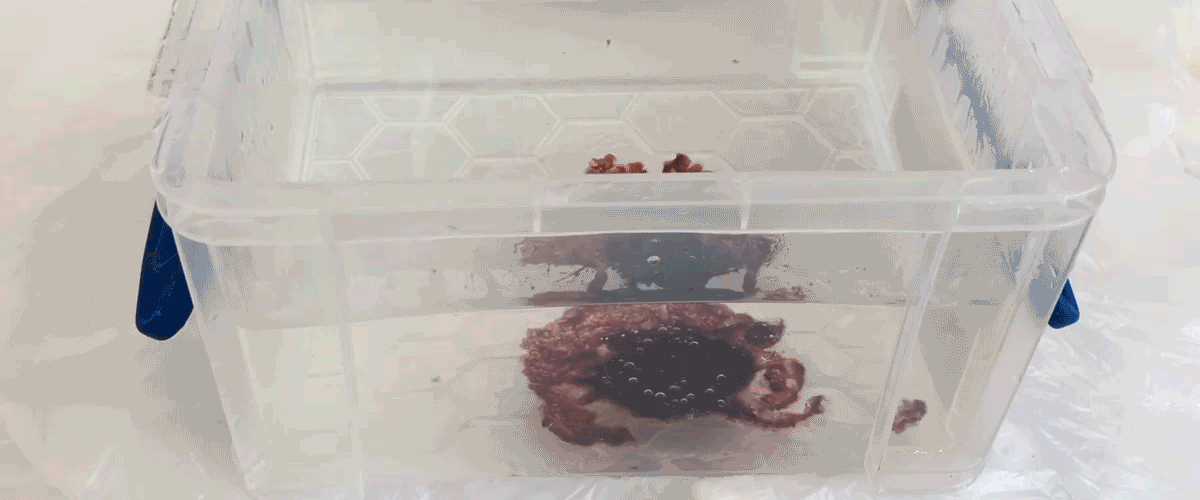
Project | Biocomposite Soft Robotics
Demonstrating a new kind of bio-based smart material actuator
splishily, splashily ...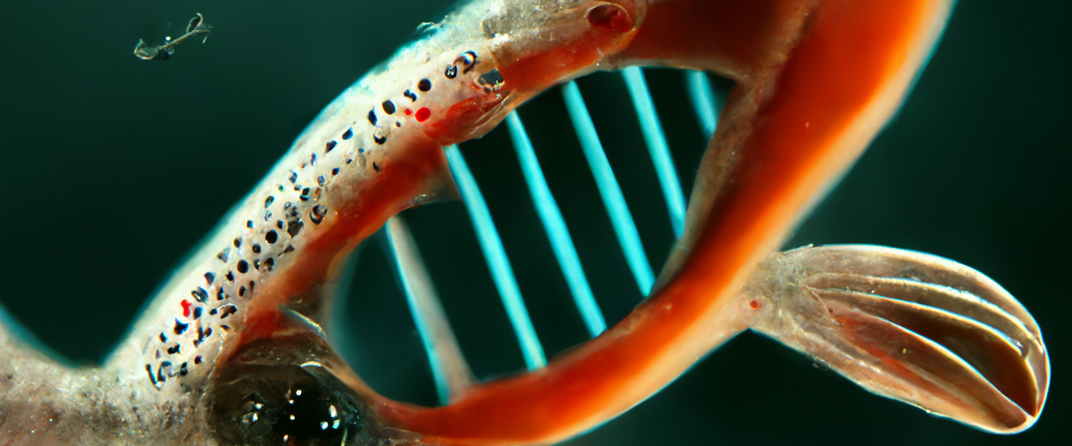


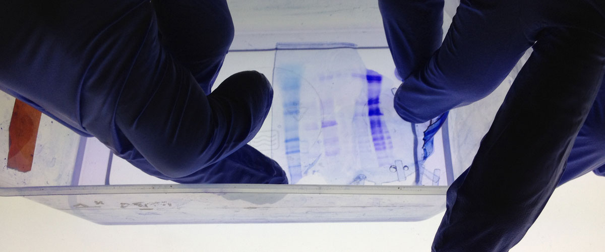
Project | Biomolecular Sensor System
Using biodesign to detect harmful agents in drinking water, and the environment that surrounds us
check it ...

News | New Publications!
Works, old and new, continue to engage the imagination

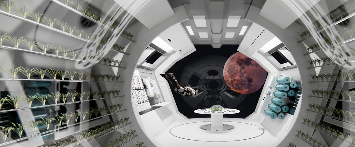
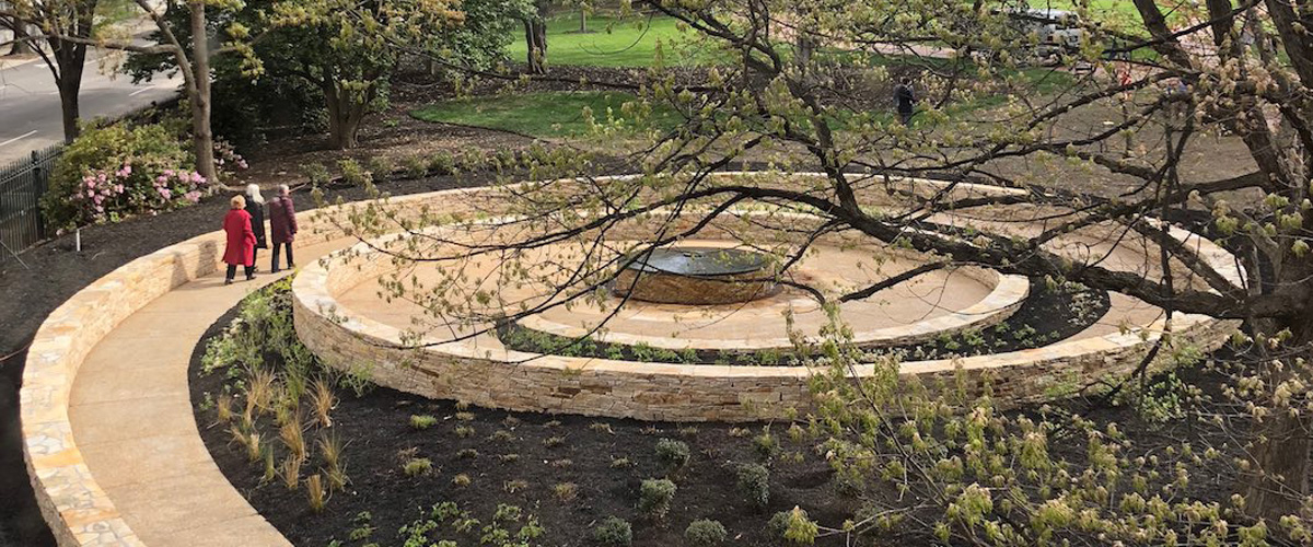
Project | The Stillest Place on Earth
A place from which we can witness the Earth spin below
spin it ...